SMART CARD-EXPLAINED

Thursday 5 December 2013
In simple words smart card is a credit card with a microprocessor.
*This is the microprocessor that is embedded in smart card. Vcc is power supply,Rst is used to reset the card communication,clk is used to provide card with a clock signal,Vpp is programming voltage,Gnd is to provide ground,I/O is serial interface as smart card uses it and C4,C8 are AUX1,AUX2 respectively and are used for USB interfaces.
*Before knowing more about smart cards let us have a look on credit cards as these smart cards are evolved to overcome the disadvantages in credit cards.
*Credit cards store information on magnetic strip line, which is easily breakable. Magnetic strip technology remains in wide use in US, however the data on stripe can easily be read, write or even can modified as stripe is not the best place to store information, we need an alternative and confidential place to store it.
*To protect the customer business in US, smart cards are introduced which will overcome the above said disadvantage.
*Smart card usually contain an embedded microprocessor, which is under gold plated contact pads and performs mathematical encryption calculations used in security function and also store additional card holder account data.
*In Europe, health insurance and banking industries use smart card extensively.
*A smart card has 8kb of RAM,346kb of ROM,256 kb of PROM and a 16 bit microprocessor
*Smart card uses a serial interface and receive power from external sources like card reader.
How it works?
*When a smart card is inserted in smartcard holder, transaction is similar to that of an ATM, but in here power goes from smart card reader(machine) to chip and switches it ON, once it is ON, it is able to conduct, an electron conversation  with chip reader. When the reader is online, the chip uses the reader to communicate to card issuer,during this time security procedure is activated that authenticates the card. A fake card would not be able to duplicate the security procedures and would be detected invalid.
*Magnetic strip information on credit card can be copied and put on fake card,  which looks exactly as valid card. The technology required to copy data  from smart card to a fake card is beyond capability of criminals, and the information sent online to authenticate the card is different for every transaction ,also to attempt to physically remove the chip from smart card would cause the chip to blow and chip cannot be used again.
*Smart card is of two types
1.       Contact smart card:
Contact area of smart card is approx. 1 sqcm,comprising of several gold plated contact pads, these pads provide electrical connectivity when inserted into reader, which is used as communication between smartcard and host(PC),these do not have batteries, power is supplied by card reader
2.       Contactless smart card
In this type of smartcard, card communication with Is powered by reader through RF induction.
Problems in using smart card:
1.The plastic card in which chip is embedded is fully flexible, so hard to maintain it.
2.As I said before, smart card is inserted into smart card holder, if the holder contains malware then it tries to know the information which makes the card  to turn invalid.
Read more ...

Working of WI-VI(WIRELESS VISION)

Saturday 23 November 2013
Hi friends,this time came up with new technology "WI-VI(Wireless Vision)".This technology uses  "WI-FI"(Wireless Fidilety) to allow user to look into the walls.This technology analyses the reflected WI-FI signals to estimate an object in a particular room,even if it is in motion we can able to detect the exact location of object.
Here in this case,the user has two antennas which generate WI-FI signals continuously with 180 degree phase difference and a single receiver.Generally a portion of WI-FI signal can penetrate in to wall.When two antennas radiate,due to 180 degree change in phase they cancel out each other without reaching at receiver when they hit any stationary objects,but when these signals hit any moving object there generates a change which will appear at the receiver,by analyzing the received signal we estimate perfect location of object.
Actually this concept is similar to RADAR(Radio detection and ranging),in which 'radio' signals are transmitted in to space to 'detect' the presence of object and 'ranging' involves knowing the exact location of object from the system,how?range or distance is speed over time,we know the speed of transmitting signal and the time taken for signal to strike the object from system(user),by this range is detected.
WI-VI systems are capable of tracking the person in a closed room.Assume that a WI-VI device is fixed outside the room,initially room is empty,when a person enters into it based on the movement of person the device is capable of showing variations i.e when he moves towards the WI-VI, signal may be in one format and when he moves away from it we can see the signal in another format.A small variations can also be grabbed by WI-VI device.

Read more ...

Introduction to Zener diode

Monday 11 November 2013
Hi friends,this time we wanna discuss about zener diode which is heavily doped diode and is specially fabricated to with stand high power dissipation.
Main application of zener diode is, it can act as a voltage regulator.
Forward characteristics of zener diode:
when high potential is applied at anode compared to cathode,then the characteristics of 
zener diode are
Negative characteristics of zener diode:
when lower potential is applied at anode compared to cathode,then the characteristics of 
zener diode are
Major concern related to zener diode is determining the state in which the zener diode is residing,there are various steps that to be followed in this process,
  1. Replace zener diode by an open circuit
  2. Find terminal voltage across the diode from N to P side,say vt
  3. If vt>vz,  zener is reverse ON  and replace it with vz
  4. If vt<vz,  zener is OFF and hence open circuit.
Consider a circuit ,
now the circuit becomes 
Terminal voltage Vt=(8*1.2)/(1+1.2)=4.3v and since Vt<Vz zener is OFF hence open circuit.
If  RL=3.6k then terminal voltage Vt=(8*3.6)/(1+3.6)=6.26v. Here Vt>Vz hence zener is reverse ON and replace zener diode with Vz=6v.
Now the question is how to place a terminal voltage,the answer is conventional direction of zener voltage is considered to be opposite to the direction of normal PN diode,because  PN diode is used in forward biased and zener diode is used in reverse biased.
For RL=3.6,the circuit becomes 
Read more ...

TRANSISTOR Disadvantages-MOSFET Advantages

Thursday 31 October 2013
Hi friends,this time i wanna talk about basic electronic devices, they are transistor and mosfet with their disadvantages and advantages respectively. Major disadvantages that i would consider for transistor are,
1.Input impedence
2.Stability
I would also explain how these two are advantages for mosfet.
1.Input impedence : 
For transistor:Any small input at the base terminal will turn transistor active and make it work (i.e as a amplifier or as a switch),which is not required at particular small input. Transistor should respond only to a reasonable input .This indicates the input impedence(Ri) of a transistor is low.Actually for CC based transistor configuration,the input impendence is upto 500k ohms,which is enough, but if transistor is biased then due to R1 and R2 the net input impedence will decrease(R1||R2||Ri).
For mosfet:Mosfet abbreviates metal oxide semiconductor field effect transistor,as the name itself indicates presence of oxide(SiO2) an insulator,which  prevents mosfet not to respond for small inputs
2.Stabilty
For transistor:We desire a fixed operating point that to in active region with Ib,Ic,Vce.The flow of small current(due to low input impedence) into BJT results in dissipation of electrical energy inform of heat.This results in rise of tempoerature which inturn increases Ic0 but Ic=(alpha)IE+Ic0,so Ic also increases.With this operating point is disturbed.It is referred as bias instability.To overcome bias instability,we have bias circuits which will stabilise the Q pont even change occured in Ic0 and temparature.Ic0 increases by 2 times for every 10 degree rise in temperature.
For mosfet:Bais instability is occured in BJT due to low input impedence,but as i said mosfet has high input impedence(due to SiO2) compared to transistor,so chances of instability is less in case of mosfet.
Read more ...

Circuit which indicates the charging level of battery

Saturday 19 October 2013
Hi friends ,As the need for rechargeable devices are increasing it is necessary to maintain the life of electronic devices which runs with  battery.Life of any rechargeable device depends upon the usage of charging capacity it has.Overcharging leads to reduce the life of device.Now a days due to overcharging many of the devices are out of work field.So if we know proper charging level of battery at every instant of time,it would help us to know whether to charge the battery or to use it.My circuit provides this features i.e when the battery is fully charged we can see a LED light glowing by this one will come to know that the battery is fully charged and has to unplug it.If not it need to be charged. Today i wanna show a circuit which will indicates the charging level of a DC storage battery.


Circuit description:
Input is an alternating voltage signal of 220v and 50hz supply,given to capacitor which is used to block DC,Stepdown transformer to reduce the signal level ,a rectifier to convert AC to DC,inverting and non inverting amplifiers,LED,1 v DC source and the battery whose charging level is to be detected.
Working:
Initially AC signal is passed through 'C' to block DC,which is fed to step down transformer to reduce the voltage signal from 220v to 13v.Now this is given to rectifier circuit for conversion process i.e from AC to DC.This constant 13V is given to non inverting terminal of opamp-1,inverting terminal is given with battery positive terminal for same opamp.Output of opamp-1 is given to inverting terminal of opamp-2 and its non inverting terminal is grounded.Output of opamp-2 is fed to LED which has -1v supply.
Operation:
case:1 Assume initially the battery has 2v in it ,V+>V-,therefore V01 is 13-2=11v,V02=-11v,since the potential at anode is much less than potential at cathode the LED doesnot glow.It means that battery is not yet fully charged.
case:2 Assume now the battery is fully charged i.e upto 13v,V+=V-,therefore V01=0,V02=0 and now the potential at anode(0v) is greater than potential at cathode(-1v),LED glows and indicates us that battery is fully charged and need to be unplugged.
*Since the ouput of rectifer is given to battery,it charges the battery when it is discharged by the user.
*Here two opamp are used,but the same work can be done with single opamp.For better explanation i has shown two.
,

Read more ...

WIRELESS ELECTRICITY-EXPLAINED

Thursday 3 October 2013
Movement of electrons (current) in free space without using any proper conduction path between two electronic devices is referred to as wireless electricity.Long before it is a dream but after a few years it will come true.
  • Everyone knew that conductor has free valence electrons, by applying proper voltage (nothing but force) these electrons move and results current(flow of electrons).

1.Actually the concept of wireless electricity has started with faraday's law.
It states that whenever a conductor is placed in magnetic field(time changing) an induced emf(electro motive force) or voltage is induced in another conductor.This is considered as base for wireless electricity. Without any proper conduction path,this induced emf will results to move electrons in another conductor.This concept resulted to discover transformer.With the transformer we are able to alter voltage from a high valve(received from station)to a value required for home appliances.This is beginning for wireless electricity.
2.Second thing I would consider is from the basics of antenna. Actually antenna is an interface between free space and transmission line that converts V/I waves into E/H waves at the transmitter and viceversa at the receiver.HOW? When a voltage(V/I) is fed at the input, due to electric field(electrons) and magnetic field(as these electrons are moving),E/H waves are released into medium, this conversion V/I into E/H process is called radiation and at the receiver E/H is converted back  to its V/I form, this process is called induction.
By adopting both radiation and induction techniques we can transmit electricity without proper conduction path between two devices.
Conclusion:From first technique we need a strong magnetic field between two wireless devices and from second technique we need an antenna for wireless transfer of electricity.
Read more ...

Software's for Win 7 homebasic and Add-on for chrome

Saturday 28 September 2013
Hi friends this time i would like to share two softwares for windows 7 home basic operating system and a Add-on for Chrome browser.
1.Software-"personalization -setupfile"
Every user of win 7 home basic will not find personalize option in the popup menu,but where as in win 7 professional , ultimate and home premium, users can have it with which one can change the wallpaper of desktop by one click.To get the personalize option for home basic ,download a setupfile "personalization" and get installed in your PC.And now you can see personalization option in popup menu.But we have still left out with "next background option",by which wallpaper changes automatically.
2.Screen Shot Add-on-"CLIPULAR"
    For chrome users,Clipular is one of the best screen shot Add-on.When Clipular is added to chrome,one can take screen shot for the tabs s/he has been working on.Screen shots of full screen or else a part can be taken which will be stored in book(Add-on book),for usage of that image(screen shot) one has to login ,save the file and use it.Since it is add-on for chrome one cannot use it outside chrome.Shortcuts are specified ,which ease its usage.
3. Software-"EPICPEN"
    Those who want to draw on screen, to specify a matter to another user. Epicpen software is useful.By using this,one can able to highlight the matter,that s/he is going to convey.By installing this software one can use a pencil,eraser and color selection.But one cannot draw straight lines or a particular shape,only zigzag lines are allowed.The file can be found at http://sourceforge.net/projects/epicpen/
Read more ...

DISPLAY DEVICES-EXPLAINED

Monday 23 September 2013
HI friends in this post we are going to learn about the various types of DISPLAY DEVICES which we had been known.In this the foremost one is 

1.CRT(Cathode ray tube):Experiments to discover more on smallest  particle "atom"(on that time)by J.J thomson, landed him to know about electron.In his experiment he noticed that a ray of particles called electrons(named by G.J stoney) were travelling from cathode to anode,he made this electrons to fall on fluorescent screen when this electrons hit the screen bright spot is produced.On their way from electron gun to screen their is chance of deflection, due to surrounding fields(as electrons are negative),to overcome this he placed horizontal and vertical deflection plates in between the space.So based upon the electrons, which hit the screen display is produced.now a days we can observe CRT's in CRO(cathode ray oscilloscope) .Next to this is 
2.LCD(liquid crystal display):Display by liquid crystals.Normally we know crystals in solid form like rochelle salt,quartz etc unlike here it is liquid crystals,means crystals which are in liquid form or in which the  molecules tend to orientate easily.Actually liquid crystals state is in between solids and liquids.As we know that even on slight increase of temperature will turn this liquid into real liquid so liquid crystal  are effected easily by electric current.Based upon this feature, applied electric current results molecules change their orientation with which display is produced.Next to this
3.LED(light emitting diodes):The diodes which emit light when they are forward biased are LED's.when we look at aluminum-gallium-arsenide(AlGaAs), in this type of semiconductor made diodes the interaction between electrons and holes is interesting , which is responsible to emit light.we knew in previous post "introduction to pn junction diode" about diode condition when no external bias is applied i.e  depletion layer is formed(electrons recombine with holes due to diffusion) on recombination electrons jump from lower orbital to higher orbital and vice versa .Electrons lose(release) energy when they jump from higher to lower orbital and needs(gains) energy to move from lower to higher orbital.The energy released in this process is in form of photons which are basic particles of light,these photons have speed and momentum but have no mass.
you can ask me, why this emission of light doesn't occur in normal Si, Ge diode,the reason is that atoms in normal diode are arranged in a manner that energy drop is relatively short which is invisible to normal eye.By release of photons in led's display is produced.Next to this
4.OLED(organic light emitting diodes):The main differences between led and Oled is the presence of organic layer present between anode and cathode of a diode.The organic layers in Oled are organic layer,conducting layer,emissive layers,the main purpose of this layers are to transport much holes from anode and much electrons from cathode, this will increases the recombination rate which in turn increases the emission of photon which are basic particles of light,this is how display is produced in Oled.

Read more ...

TRANSMISSION MEDIA

Wednesday 11 September 2013
Now a days communication is necessary in every field and to communicate a transmission media is needed. Transmission media is classified into two types.
·         Wire communication (a connection between transmitter and receiver.)
·         Wireless communication (no connection between transmitter and receiver.)
1.                                                          In case of wire line communication, nonelectrical signals are converted into electrical signals                         at the entry and these electrical signals(voltage,current) are transmitted with the help of                                   conductor.The device which transforms it is called the “Transducer”

There are 3 major and well known types of wire communication
·         COAXIAL CABLE:
*It is kind of copper cable mostly used by cable tv companies between communicating antenna and user home tv set and is applied by telephone companies from their offices to poles.
*This cable has three layers enclosed in it, inner layer is conducting copper wire and  two outer layers are used to protect the conducting(cu wire) path from outer damages.
*Major disadvantage regarding this cable is electromagnetic induction
HOW? Here it is said that electrical signals are transmitted by inner cu layer ,it means we have electric field and as these electrons are flowing(current) we have magnetic field around the conductor.so both fields exists. whenever another conductor is brought near to it, we may have collision and there is chance of loss of information.
·         TWISTED PAIR:
*To overcome the loss of information in the coaxial cable Twisted pair cable was introduced as name itself indicates pair of wires are twisted one, to collapse electromagnetic interference.
*It is ordinary wire that connects home and many business computers. To reduce  cross talk and electromagnetic induction between pairs of  wires ,two insulated cu wires are twisted. These are sometime enclosed in single cable this acts as a shield for twisted pair cable.
*For secure information this shield acts as ground and is called as shield twisted pair cable and for home transmit information this shield acts as unshielded and is called unshielded twisted pair cable.
*Major advantage is twisted pair is cheaper than coaxial cable and it overcomes EM induction.
*Disadvantage is slow transfer of information.
·         OPTICAL FIBER:
Up to this security is enough and every one needed the speed and thought of using the light as source to transmit the information as we knew that the speed of light is 3*108m/sec. Based on this technique optical fibre was designed. Similar to coaxial cable it also has 3 layers, outer one is buffer or sheath,middle one is cladding and the inner one where the light is gonna transmit is core. For proper transmission refractive index of core must be slightly greater than cladding. To know how light transmits in the core one should know about the critical angle and total internal reflection.
      *critical angle: When a wave is transmitting from one medium to another medium of different refractive indices and if wave incident angle is greater than 90 degrees this angle is referred as critical angle
      *Total internal reflection: When angle of incident is equal to critical angle then no reflection occurs only refraction into medium.
*By using these light parameters transmission is done in optical fiber. *Major advantages is Optical fiber carries much more information than normal cu wire and is not subjected to EM interference, so most telephone companies long distances lines are made of optical fibers by use of Repeaters at regular distances.
 2.     In case of wireless communication no wired media is present between transmitter and receiver. Here communication is by EM waves HOW? As I said before around a conductor both fields exists and these EM waves are necessary for communication.
The first wireless transmission went on air in early 20th century using morse code. Later by modulation it made possible for transmitting voices and music via wireless.
Modes:
Wireless communication can be via,
·         Radio communication(Radio frequency)
·         Microwave communication(high frequency)
·         Infrared communication
·         Ultrasonic communication.are made of optical fibers by use of Repeaters at regular distances.
1.                                    
Read more ...

Li-Fi(Light Fidelity) future wireless communication

Monday 19 August 2013
In future it is suspected that every light bulb will be replaced by LED's the reason is LI-FI .Li-Fi  is acronym for light fidelity.The word fidelity means the ability of the receiver to reproduce all the signals.Light fidelity indicates transmission of data or information through light or illumination. The inventor defines it simply if LED is ON you transmit a digital '1' and if it is OFF you transmit a digital '0'.Li-Fi is the  next version to Wi-Fi(wireless fidelity) as it overcomes some of the limitations of Wi-Fi like speed,application areas like medical and in aircraft,outreach in remote areas etc.
NEED FOR LI-FI:
When you are using mobile phone or pc connected to wireless internet we have to compete for bandwidth and sometimes we get frustrated with slow speeds when more than one devices are connected. To solve this problem german scientist Herald Hass found an alternative way and he calls it with "data through illumination".He conveys that in future communication is done through Light in a room.
HOW IT GONNA WORK?
Li-Fi is transmission of data through illumination by taking fiber out of fiber optics by sending data through LED(light emitting diodes) light bulb that varies its intensity faster than human eye can follow.As said before  if LED is ON you transmit a digital '1' and if it is OFF you transmit a digital '0.As the reaction time of LED's to respond to the changes is very fast the transmission of data will also be fast. Theoretical calculations had proven that the rate of data transmission would be 224 giga bits per second.
*The requirements to adopt this technology are some LED's and controller that code data into those LED's
*Since it just uses light ,it can be used safely in aircraft and in hospitals that are prone to interference from radio waves.
*Simply radio waves are replaced by light waves in new method called Li-Fi.
*This method of using rapid waves of light to transmit information wirelessly is referred as Visible Light Communication(VLC) the transmitting frequency in VLC is around is 400Thz to 800Thz.
MAJOR APPLICATION AREAS OF LIFI:
1.IN FIELD OF MEDICAL:
Most hospitals donot allow Wi-Fi to enter into operating rooms due to radiation concerns and even it is lagged by some other cellphones or ipods, but communication is necessary in operation theaters  to treat patients.
LI-FI overcomes it.I think many of we know about the properties of light like inteference,diffraction ,polarization etc.Diffraction means bending up of light around the edges or obstacles.This property helps LI-FI to increase its efficiency.
2.AIRLINES: Where radio waves are not much efficient.
3.OUTREACH IN REMOTE AREAS:As the equipment for Wi-Fi is necessary, it is not possible to lay plant anywhere but since here in LI-FI it is through light we just need LED's and a controller.
4.UNDERSEAS:As it is difficult to lay optical fibers beneath water, it is better to communicate with help of light and as salt water is good conductor of electricity it is easy to work with LI-FI
5.FAST TRANSFER OF INFORMATION:As LED's ON and OFF very quickly which gives nice opportunities for fast transmitting the data.  
Read more ...

chemistry concepts

Saturday 17 August 2013
                           Universe is composed of  matter,during vedic period in india ,maharshi kanada proposed that matter is composed of smallest particles such as "anu" and "paramanu". later a greek philospher proposed that matter consists of smallest particles called "Atoms" meaning indivisible , Atoms combine to form "compound atoms",which later on called as molecules. According to modern theories Atoms contain positive charged nucleus and negatively charged electrons. Nucleus further contain protons which are positively charged and neutrons which are neutral, combinely both protons and neutrons are called Nucleons. Mass of electron is negligable while mass of proton is 1837 times of electrons. J.J Thomson is the person who discovered the cathode rays(electrons which are travelling from cathode to anode and these are invisible.G.J Stoney named these cathode rays as "electrons".
  Two types of forces are present in atom a)force of attraction between the electrons and protons(Attractive force).This force pulls the electrons towards the nuclues. second type of force is b)the revolving electrons experience a centrifugal force directed away from the moving path of electrons.This force pulls away the electrons from nucleus ,since these two forces are equal and opposite ATOM is stable.
IF THESE ATOMS ARE STABLE WHY THEY COMBINE?
It is known that inert gases like Ne(10),Ar(18),Kr(36) have stable electronic configuration and have no tendency to combine with other atoms.Elements like fluorine(9),chlorine(17) are very reactive as they are short of one or two.Similarly atoms of Alkali metals like Li(3),Na(11),K(19) are very reactive and form numerous compounds.
WHY SOME ARE REACTIVE AND SOME OTHER NOT?
In the above paragraph i used the word "electronic configuration",it is defined as systematic arrangement of electrons in the atomic orbits.The maximum number of electrons present in each orbit is generally given by 2nsquare.(n=number of orbit) i.e 1st orbit -2,2nd orbit-8,3rd orbit-18...
*Electrons present in the outer most orbit of an atom are known as valence electrons and based on these atoms are said to be reactive or not.Now observe electronic configuration of inert gases they have 8 electrons in their outermost orbit except helium(2) all are stable in inert gases.
*Halogens have 7 electrons in outermost orbit.Normally every atom has tendency to attain nearest noble gas configuration and become stable,As they are 1 electron short they combine with another atom to have 8 electrons which provides them with much stability.
This is perfect reason for "chemical bonding".Atoms combine to form molecules so "molecules are much stable than atoms".
Read more ...

Ways to improve system performance

Friday 26 July 2013

Introduction:
Now a day’s computer plays a major role in our lives. In any work there is a need of computer.so we have to take care of the system i.e. we have to maintain it properly without decreasing its performance so that we can complete our works fast. Most of the people assume that the amount of RAM memory increases the system performance. It is not true all the time .suppose take two systems A & B having the RAM memory 2GB and 4GB. If both A & B works on a two tasks say one is web browser and media player. Both processes take maximum of 50MB usage of RAM. In this case the accessing speed of A and B are same (provided that they both maintain the system properly). When the difference comes into picture is if the processes take beyond 1.5GB of RAM then ‘A’ gets problem. For official works there is no difference in the processing speed of A & B even though B is having 2GB more than A. when the difference occurs is in maintenance.
In this paper I want to tell about the ways to improve the system performance and the tools required to improve the system performance.
1.  Disk cleanup
Windows utility free up disk space on computer harddrive.
*It first searches and analyses for files that are no longer of any use and removes unnecessary files.They are
·         Compression of old files
·         Temporary Internet files
·         Temporary Windows files
·         Downloaded program files
·         Recycle Bin
·         Removal of unused applications or optional Windows components
·         Setup log files
·         Off-line files
In windows7 for getting Disk Cleanup
Go to Start menu >type Disk Cleanup

Disk cleanup involves the deletion of temporary files like temporary internet files and temporary program files which are useless for the system. And also disk cleanup cleans thumbnails , error reporting files, and it also cleans up the recycle bin
2.Disk Defragmenter:
Disk defragmenter involves reallocation of memory.
*Fragmentation makes your hard disk to do extra work and slow down your PC.Removable storage devices can also fragmented.disk defragmenter rearranges fragmented data so your devices and drives can work efficiently.
*First we have a option for analysing each hard drive if it is greater than 10% then defragmentation is must.
*Suppose if hard disk contains errors then it is not possible to defragment it,first we have to clean the errors in respective hard disk.
Windows 7
Windows 7 is different from the other versions as the user is able to follow the defragmentation percentage as it run. It will not defragment a solid-state drive, as SSDs don't require defragmentation and doing so reduces their limited lifespan.
In windows7 for defragmentation
Go to Start menu>type disk defragmentation 

I.e. the storage of the files in a memory is in order after defragmentation. Hence accessing of the memory is very easy.so performance of the system will increase. 
3.Deleting the Prefetch files:

When you open any window in your PC ,a file or directive will store or copy of program in a folder called Prefetch.

In windows7 for prefetch folder     Go to Run>type Prefetch    

 Or    Key board Shortcut is Windows button + R And then you have to run the command called Prefetch then prefetch folder is opend Or  The path for the folder is My Computer\X:\windows\Prefetch
Where X is the disk where the windows is installed generally it is local disk C 

4.Deletion of Temp files:
In computing, a temporary folder or temporary directory is a directory used to hold temporary files. Many operating systems and some software automatically delete the contents of this directory at boot up or at regular intervals.


5.Remove spyware, and protect your computer from viruses using Microsoft Security Essentials
While you're busy surfing the web, spyware and other types of malicious software (also known as malware) are collecting personal information about you, often without your knowledge. The result is that your personal information could possibly be compromised. At the same time, spyware and malware can slow down your computer. Download Microsoft Security Essentials for free to help guard your system in the future from viruses, spyware, adware, and other malware. Microsoft Security Essentials acts as a spyware removal tool and includes automatic updates to help keep your system running efficiently and to help protect it from emerging threats.

6. Turn Ready Boost on or off for a storage device:

ReadyBoost can speed up your computer by using storage space on most USB flash drives and flash memory cards.
To turn ReadyBoost on or off
1.      Plug a flash drive or flash memory card into your computer.
2.      In the Autoplay dialog box, under General options, click Speed up my system.
3.      In the Properties dialog box, click the ReadyBoost tab, and then do one of the following:
·         To turn ReadyBoost off, click Do not use this device.
·         To use the maximum available space on the flash drive or memory card for ReadyBoost, click Dedicate this device to ReadyBoost. Windows will leave any files already stored on the device, but it'll use the rest to boost your system speed.
·         To use less than the maximum available space on the device for ReadyBoost, click Use this device, and then move the slider to choose the amount of available space on the device you want to use.
4.      Click OK.

7. Check hard disk and RAM for errors
Whenever a program you're using crashes, your computer may create errors on your hard disk. These errors will eventually slow your computer to a crawl.
The good news is that Windows includes a Check Disk program. Check Disk corrects these types of errors on your hard disk, resulting in better PC performance.
About once every week, you should run the Check Disk utility. While Check Disk runs, a black window will open. If you happen to be working at your computer when the window opens, you can ignore it. The window will automatically disappear when Check Disk is complete.
Note: You must be logged on as an administrator to perform these steps. If you aren't logged on as an administrator, you can only change settings that apply to your user account.

For RAM Errors : Run,type Memory disgnostic press enter,then you can find any errors crept in your RAM which are responsible for slowing down your computer.
8.Disable the unwanted programs in the startup :
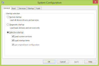
When starting up your system, there’s several programs which starts up with it. Disabling unwanted programs such as Windows Live Messenger will increase the general speed of your PC. Additionally, it’ll also result in your boot time being faster.
in windows7 operating system for disabling the unwanted programs in startup
Run the command called msconfig


9.Uninstall the unwanted programs:

When a program is installed, it creates connection between program and OS, even if you don’t use program, these can slow down your PC. If you have original program setup you can uninstall it now itself.

10.Common and minor mistakes we do in daily usage of system which intern affects the system performance   

  1.  Desktop is filled with the shortcuts, files and icons.
  2. Unwanted programs are installed in the primary memory
  3. More apps are pin to taskbar
  4.  Recycle bin contains the files.
  5. Using applications like gadgets, rocket dock, and lion skin packs
  6. Turn off the system by pressing the power button
  7. Using of large size icons.
  8. Not updating the spyware (Anti -Virus).

Conclusion:
By using above techniques we can improve the system performance .even a minor mistake can affect the system a lot. It is not the matter how much RAM memory (main memory) we have, how we maintain the system is important.


Read more ...

Basics in Electronics

Wednesday 24 July 2013
1.Purpose of Tank circuit.
      To amplify a selective range of frequency this circuit is used.Output impedence(Rc) is replaced by tank circuit
Operation:When initially C is charged,it finds path to discharge through L it stores the energy in form of magnetic field.Now according to lenz law,magnetic field start collapsing and this in turn charges the capacitor in opposite direction.After some time capacitor fully charges.Here magnetic energy is converted back to eletrostatic energy.Now the capacitor again starts discharging through inductor L .This capacitor produces alternating current in tank circuit.
By selecting the L and C and placing it in f=1/(2pi root(LC)),We can fix the frequency and at a specified frequency we can amplify the signals.
2.Why in P-type semiconductor majority charge carries are holes and in N-type semiconductor majority charge carries are electrons
Semiconductors like silicon and germanium belong to 4th group of periodic table.To form a P-type semiconductor silicon(4 valence electrons)  is doped with 3rd group elements like berillium(3 valence electrons) so one electron is short.so in P-type majority charge carries are holes(positive charge).In the same manner
To form N-type semiconductor silicon(4 valence electrons) is doped with 5th group elements like phosphorus(5 valence electrons) so one electron is more.so in N-type majority charge carries are electrons(negative charge)
3.why cant capacitor stores only DC but not AC
AC signal is which varies accordingly with time, and has amplitude in both positive and negative levels like a sine wave.Capacitor also does charging for the positive cycle of AC and discharges for negative cycle of AC so net is zero. 
4.Transistors disadvantages
a.Input impedence : Rb for the transistor is low.Actually the input impedence of CC configuration is around 500kohms which is sufficient.But since we place R1,R2 for biasing purpose(to place the transistor to act as an amplifier)the net impedence decreases(R2//R1//Ri).To overcome this situation we have 2 techniques they are Darlington connection and Bootstrap emitter follower.But since we cant adopt this type of situations we consider this as a disadvantage because a week signal should not drive the transistor.
b.Stability:This is also one of the reason to implement the FET(field effect transistor).We desire a fixed operating point that to in active region with Ib,Ic,Vce. The flow of I2 into BJT results in dissipation of electrical energy in form of heat . That results in rise of temperature which in turn increases Ic0 but Ic depends upon Ic0. so Ic also increases and operating point is disturbed, it is referred as Bias Instability.
5.Why in BJT conduction is from Emitter to Collector and not viceversa.
First off all one should remember that BJT is not a symmetrical device (Emitter and Collector regions are not interchangable).As we know BJT provides two configurations i.e NPN and PNP.In any of these  Base(middle region) is lightly doped to have small recombination ,Emitter is heavily doped  and collector is moderately doped.So normally when base current is applied,conduction is carried from higher region to a lower region(process known as Diffusion) since emitter is heavily doped and collector is moderately doped,conduction is from Emitter to Collector.This is reason behind why in  BJT conduction is from Emitter to Collector and not viceversa.
6.Why P mos is ON for logic 0 , OFF for logic 1 and N mos is ON for logic 1,OFF for logic 0
When Vgs is positive there is force of attraction between gate(positive) terminal and N majority charge carriers electrons(negative) so no channel is formed between two highly doped N regions.By this we can say that P mos will be in OFF state when logic 1(high) is applied.
When Vgs is 0 or negative due to force of repulsion between gate(negative)and N majority carriers electrons(negative) and channel formation takes place which leads to conduction from source to drain.So P mos conducts when logic 0 is applied.
Similar action is followed in N mos

 When Vgs is positive there is force of repulsion between gate(positive) terminal and P majority charge carriers holes(positive) so  channel is formed between two highly doped P regions.By this we can say that N mos will be in ON state when logic 1(high) is applied.
When Vgs is 0 or negative due to force of attraction between gate(negative)and P majority carriers holes(positive) and no channel formation takes place between two highly doped P regions.So N mos doesn't conducts when logic 0 is applied.
7.Why P mos connected in pull up network where as N mos connected in pull down network
or
source of P mos is connected to Vdd and source of N mos connected to Vss
As i said before P mos will be in ON state when logic 0 is applied i.e Vgs is negative this happens when gate terminal is negative and source is positive,So in P mos source is always connected to Vdd which is positive.Coming to N mos it will be in ON  state when logic 1 is applied i.e Vgs is positive this happens when gate terminal is positive and source is negative,So in N mos source is always connected to Vss which is negative.This is reason why P mos is connected in pull up network and N mos is connected in pull down network.


Read more ...